RepRap Transistor / Polymer Doping
Posted by savecore
|
RepRap Transistor / Polymer Doping July 05, 2007 11:13AM |
Registered: 16 years ago Posts: 23 |
Okay, I'd like to start a thread about a RepRap transistor. I know the priority / viability of a Reprap transistor is arguable (ie. "If we get PCB's to print using copper, we don't need in-house transistors for awhile", etc). I am not arguing with these points as they are valid ones.
Instead, I'd like this thread to be a discussion of the various polymer technology which could be used to implement a theoretical RepRap transistor (or diode), with an eye to the next generation of machines.
As most of you are aware, transistors are made of silicon (a semiconductor) and have three regions of silicon which are "doped" with ions to make the N or P components. "The emitter is heavily doped, while the collector is lightly doped, allowing a large reverse bias voltage to be applied before the collector
Edited 2 time(s). Last edit at 07/05/2007 11:44AM by savecore.
|
Re: RepRap Transistor / Polymer Doping July 05, 2007 11:39AM |
Registered: 16 years ago Posts: 23 |
Conjugated Polymers: Electronic Conductors
[mighty.caltech.edu]
"the [property] is simply a boundary between two moieties of equal energy -- the infinite conjugation chain on either side -- [the charge] can migrate in either direction without affecting the energy of the backbone, provided that there is no significant energy barrier to the process. It is this charge carrier mobility that leads to the high conductivity of these polymers."
. . .
"Consequently, conjugated polymers are insulators in their neutral state and no intrinsically conducting organic polymer is known at this time. A polymer can be made conductive by oxidation (p-doping) and/or, less frequently, reduction (n-doping) of the polymer either by chemical or electrochemical means, generating the mobile charge carriers described earlier."
Edited 2 time(s). Last edit at 07/05/2007 02:46PM by savecore.
|
Re: RepRap Transistor / Polymer Doping July 05, 2007 12:00PM |
Registered: 16 years ago Posts: 23 |
High-Resolution Inkjet Printing of All-Polymer Transistor Circuits
Science 15 December 2000:
Vol. 290. no. 5499, pp. 2123 - 2126
DOI: 10.1126/science.290.5499.2123
H. Sirringhaus,1* T. Kawase,1dagger R. H. Friend,1* T. Shimoda,2 M. Inbasekaran,3 W. Wu,3 E. P. Woo3
Direct printing of functional electronic materials may provide a new route to low-cost fabrication of integrated circuits. However, to be useful it must allow continuous manufacturing of all circuit components by successive solution deposition and printing steps in the same environment. We demonstrate direct inkjet printing of complete transistor circuits, including via-hole interconnections based on solution-processed polymer conductors, insulators, and self-organizing semiconductors. We show that the use of substrate surface energy patterning to direct the flow of water-based conducting polymer inkjet droplets enables high-resolution definition of practical channel lengths of 5 micrometers. High mobilities of 0.02 square centimeters per volt second and on-off current switching ratios of 105 were achieved.
1 Cavendish Laboratory, University of Cambridge, Madingley Road, Cambridge CB3 OHE, UK.
2 Base Technology Research Center, Seiko-Epson Corporation, 3-5-3 Owa, Suwa-Shi, Nagano-Ken 392, Japan.
3 The Dow Chemical Company, Midland, MI 48674, USA.
* To whom correspondence should be addressed. E-mail: hs220@phy.cam.ac.uk
dagger Also at Epson Cambridge Laboratory, 8c King's Parade, Cambridge CB2 1SJ, UK.
THIS ARTICLE HAS BEEN CITED BY OTHER ARTICLES:
Jumping Nanodroplets.
A. Habenicht, M. Olapinski, F. Burmeister, P. Leiderer, and J. Boneberg (2005)
Science 309, 2043-2045
From the Cover: Conformable, flexible, large-area networks of pressure and thermal sensors with organic transistor active matrixes.
T. Someya, Y. Kato, T. Sekitani, S. Iba, Y. Noguchi, Y. Murase, H. Kawaguchi, and T. Sakurai (2005)
PNAS 102, 12321-12325
A large-area, flexible pressure sensor matrix with organic field-effect transistors for artificial skin applications.
T. Someya, T. Sekitani, S. Iba, Y. Kato, H. Kawaguchi, and T. Sakurai (2004)
PNAS 101, 9966-9970
Elastomeric Transistor Stamps: Reversible Probing of Charge Transport in Organic Crystals.
V. C. Sundar, J. Zaumseil, V. Podzorov, E. Menard, R. L. Willett, T. Someya, M. E. Gershenson, and J. A. Rogers (2004)
Science 303, 1644-1646
Templating Organic Semiconductors via Self-Assembly of Polymer Colloids.
R. Mezzenga, J. Ruokolainen, G. H. Fredrickson, E. J. Kramer, D. Moses, A. J. Heeger, and O. Ikkala (2003)
Science 299, 1872-1874
Self-Aligned, Vertical-Channel, Polymer Field-Effect Transistors.
N. Stutzmann, R. H. Friend, and H. Sirringhaus (2003)
Science 299, 1881-1884
Photoexcited breathers in conjugated polyenes: An excited-state molecular dynamics study.
S. Tretiak, A. Saxena, R. L. Martin, and A. R. Bishop (2003)
PNAS 100, 2185-2190
Soft, conformable electrical contacts for organic semiconductors: High-resolution plastic circuits by lamination.
Y.-L. Loo, T. Someya, K. W. Baldwin, Z. Bao, P. Ho, A. Dodabalapur, H. E. Katz, and J. A. Rogers (2002)
PNAS 99, 10252-10256
Organic semiconductors: A theoretical characterization of the basic parameters governing charge transport.
J. L. Bredas, J. P. Calbert, D. A. da Silva Filho, and J. Cornil (2002)
PNAS 99, 5804-5809
Supramolecular Chemistry And Self-assembly Special Feature: Beyond molecules: Self-assembly of mesoscopic and macroscopic components.
G. M. Whitesides and M. Boncheva (2002)
PNAS 99, 4769-4774
Organic semiconductors: A theoretical characterization of the basic parameters governing charge transport.
J. L. Bredas, J. P. Calbert, D. A. da Silva Filho, and J. Cornil (2002)
PNAS 99, 5804-5809
|
Re: RepRap Transistor / Polymer Doping July 06, 2007 12:36PM |
Registered: 16 years ago Posts: 23 |
|
Re: RepRap Transistor / Polymer Doping July 06, 2007 05:31PM |
Registered: 16 years ago Posts: 23 |
A polymer transistor circuit using PDHTT
Krumm, J.; Eckert, E.; Glauert, W.H.; Ullmann, A.; Fix, W.; Clemens, W.
Electron Device Letters, IEEE
Volume 25, Issue 6, June 2004 Page(s): 399 - 401
Digital Object Identifier 10.1109/LED.2004.829669
Summary: A digital circuit using polymer thin-film transistors on polyester substrate is presented. The circuit consists of 171 transistors and converts a parallel word of four bits into a serial bit sequence by use of gates and flip-flops with level shifters. The integrated clock generator runs at oscillation frequencies of approximately 200 Hz with supply voltages of -25 V/+12 V. The polymer poly(3,3''-dihexyl-2,2':5',2''-terthiophene) (PDHTT) is used as semiconducting material. Measurement results for the circuit demonstrate that PDHTT can be used for digital polymer circuits.
|
Re: RepRap Transistor / Polymer Doping July 06, 2007 05:47PM |
Registered: 16 years ago Posts: 23 |
|
Re: RepRap Transistor / Polymer Doping July 06, 2007 05:50PM |
Registered: 16 years ago Posts: 23 |
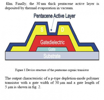
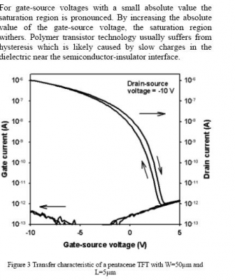
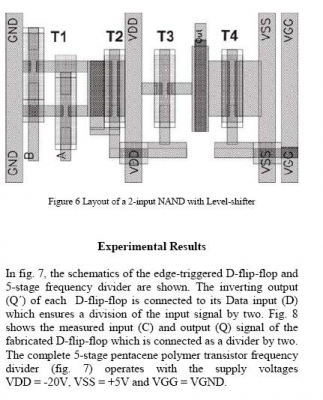
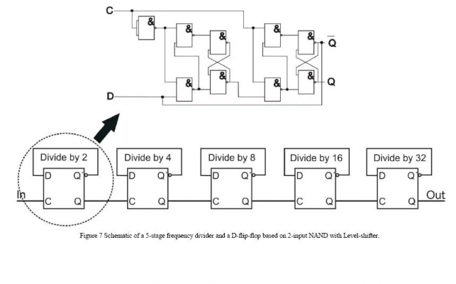
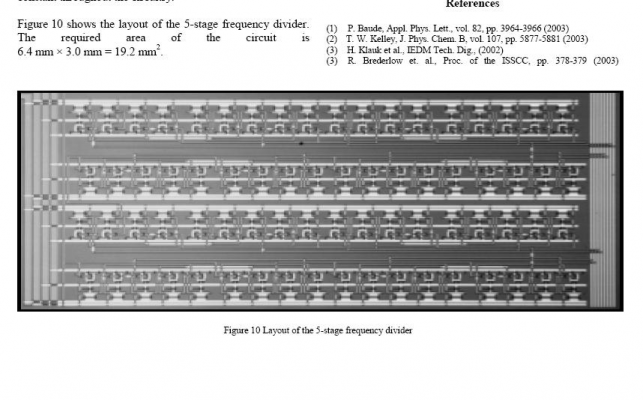
Realization of a 5-stage divider circuitry in p-type polymer transistor technology
Lackner, C.; Klauk, H.; Gut, W.; Halik, M.; Spilka, R.; Zschieschang, U.; Tanda, A.; Eder, F.; Rohde, D.; Ostermann, T.; Schmid, G.
Electron Devices Meeting, 2005. IEDM Technical Digest. IEEE International
Volume , Issue , 5-7 Dec. 2005 Page(s): 113 - 116
Digital Object Identifier 10.1109/IEDM.2005.1609281
Abstract
In this paper, we present the realization of a 5-stage divider
circuitry in a p-type polymer transistor technology using thin
film transistors with pentacene as active layer. The supply
voltage of the circuits is
|
Re: RepRap Transistor / Polymer Doping July 06, 2007 05:55PM |
Registered: 16 years ago Posts: 23 |
|
Re: RepRap Transistor / Polymer Doping July 06, 2007 06:06PM |
Registered: 16 years ago Posts: 23 |
Too big to attach the pdf, here's the important figures from the paper. This is the 0day.
|
Re: RepRap Transistor / Polymer Doping July 06, 2007 06:16PM |
Registered: 16 years ago Posts: 23 |
Everyone seems to like *thiophene as a semiconducting polymer!
High mobility, low voltage polymer transistor
Hyewon Kanga, Keon-kook Hana, Jeong-Eun Parka and Hong H. Lee
Corresponding Author Contact Information, a, E-mail The Corresponding Author
aSchool of Chemical Engineering, Seoul National University, Seoul 151-744, Republic of Korea
Received 29 January 2007; revised 3 March 2007; accepted 7 March 2007. Available online 19 March 2007.
Abstract
We introduce a polymer transistor that operates with low supply voltage and yet has a field-effect mobility higher than the mobilities reported for low voltage polymer transistors. A simple plasma oxidation of the gate metal to form a thin (3.74 nm) top metal oxide layer in the gate metal is involved in the fabrication that acts as the gate dielectric. With ultrathin gate dielectrics, the variation in the dielectric thickness and the surface roughness scattering can severely limit the mobility attainable. The plasma oxidation under certain conditions produces a very smooth oxide surface, leading to the high mobility.
Keywords: Organic thin-film transistor; Low-voltage operation; Poly(3-hexylthiophene); Aluminum oxide; Plasma oxidation; High mobility
PACS classification codes: 73.40.Qv; 73.61.Ng; 85.30.Tv
Corresponding Author Contact Information
Corresponding author. Tel.: +82 2 880 7403; fax: +82 2 878 5043
Edited 1 time(s). Last edit at 07/06/2007 06:29PM by savecore.
|
Re: RepRap Transistor / Polymer Doping July 11, 2007 10:46PM |
Registered: 16 years ago Posts: 23 |
This is my last post on this thread for the time being. You are advised to download these PDF files, even if you do not understand them. The technology mentioned is probably two RepRap generations away, but what is important is to realize THIS IS POSSIBLE, and this information has value.
Dr. Boyer has alluded to what is rapidly becoming reality... The new paradigm is
NATURAL RESOURCES and INFORMATION
Let's make these fuckers multiply.
Dr. Boyer has alluded to what is rapidly becoming reality... The new paradigm is
NATURAL RESOURCES and INFORMATION
Let's make these fuckers multiply.
Sorry, only registered users may post in this forum.


