DIY PCBs double sided toner transfer
Release status: experimental

| Description | How To: Toner Transfer DIY PCB - by NoobMan (MTG)
|
| License | |
| Author | |
| Contributors | |
| Based-on | |
| Categories | |
| CAD Models | |
| External Link |
Disclaimer:
- Please understand, whenever possible, by all means, buy a commercial pcb. It is higly reccomended. Making your own will always mean alot of time lost, will end up costing more, and will definatelly look worse. Only your time lost (and it will be alot!) should worth more than the usual pcb price. Consider time lost on eagle and image optimizations, then basically 2-3-4 attempts at least made to garbage before you get an usable image, etching each time, consumables, drilling time, vias soldering time, etc. There is no chance anyone will make a diy pcb cheaper and better than a commercial one. Bottom line any commercial pcb is well worth 10x times its price in full. I consider making your own pcb, as a last resort solution only.
Nah. It is ideologically more pure, or rather,
just much more fun to etch your own. --Sebastien Bailard 11:24, 22 November 2010 (UTC)
- I try to be funny: only because i have already tried to be good in electronics and pcb makings and i failed hard at that ^^.
- This is not meant to be exhaustive on the topic, but merely to provide an idea for peoples doing their own pcbs can share mistakes and tips. Ofc the files should work with photo method aswell.
- The reason this page is on user and not wiki is because i wouldn't recommend it myself to most of the peoples starting Repraps.
 No worries, I'm probably going to move it to its own page at some point,
 after which it may be official documentation.
 --Sebastien Bailard 10:29, 20 November 2010 (UTC)
 --<NoobMan> anything you want - just let me know where so i can polish it further from time to time; i will stop my incremental changes meanwhile;
 also i tried to put the pictures in the middle so they can be bigger but i didnt figured how - i'm afraid i am just a noob about wiki edits and such.
- This process requires specific tools and skills, and further more, i would say it is not for the average DIY person. The "experimental" tag is there not because this doesnt work, but because this is more or less "eperimental" depending on a person tools, skills, ability to learn, etc. Ultimatelly everything is such, but beyond all reasoning, i dont want to lure peoples into nerve consuming tasks and situations they wouldnt like. Bottom line: when you start something like this, be well aware of all aspects. First aspect being that you are on your own. Second being that unless you already have the tools and already know what to do, then you are most probably better off with just buying a commercial set of electronics. Sincerely it would of been better for me also, but i just happen to like doing stuff like this.
Contents
Tools and some general tips on DIY pcbs
Tools required:
- laser printer (black and white) and right kind of transfer media/paper (primarily inkjet photo paper, but there are many substitutes);
- reasonably powerful light source (to register the top and bottom layers and fix them together);
- copper clad boards and etching chemicals + drill press with drill bits (0.8mm, 1.0mm, etc);
- and etching tank (or replaced by a sponge and a pair of gloves);
- solering iron with fine tip, prefferably at least analogue thermostated (for making vias and populating the board) and soldering consumables (solder, flux, wick, etc);
The most important tool is the temperature controlled soldering iron with fine tip. Also some magnification tool is highly recommended.
The general soldering technique is to have the iron on the part and gradually feed solder wire into the pool until the pool reaches desired shape/form/mass. Shape, aspect and coverage of the solder joint is standardized for some components and packages, but generally allows a very high grade of error. In most cases that should be the last stage of the soldering, but however, before that one needs to "tackle" the smd and position it and fix it in place. I generally resort to making a solder ball on the tip of the iron - this way i can use the other hand to hold part in place.
I did the EC22 board with a 2mm tip, but 1mm or even 0.4mm tips are much better. There is an important relation between the iron tip and the width of the solder. Basically the diameter of the solder has to be smaller than the tip. This allows the formation of a sphere of melted solder on the tip of the iron. If the solder diameter is higher than the tip, the solder will still be on the tip, but will not be a "sphere" and will not be exactly on top of the tip, but instead will be around it. As a sidenote, using the iron tip with the sphere of solder like that has 2 caveats: 1) the resin in the solder will be burned before touching the parts, which means flux is highly recommended (use only "no-clean" flux which means it doesnt need to be cleaned after); and 2) finer the tip => smaller the diameter of the solder (+more hand movement) => smaller the solder sphere on the tip (in few cases means more repetition).
For example of this "technique", a 0.4mm tip means using solder of 0.25mm, and with magnification it allows an impressive degree of miniaturization, but increases the hand movement alot and decreases the productivity, although also decreases the chances of solder bridges in some packages. Using a 1.0mm tip allows use of 0.5mm solder and speed increases a little. I would say 1.0mm tip and 0.5mm solder are closer to general use in Reprap electronics (the actual diameter is 0.5~0.54mm just different notations). The 0.4-0.5mm has more value in case of 0.5mm pitch packages, but none of those are present in current gen 3 electronics.
There are alot of good nice tutorials and explanations on the internet about soldering smd, youtube has plenty.
Get some background information of the process that you intend to do
For people who havent done this yet, before anything, get a background of the process you intend to use. http://www.Youtube.com is full witj a lot of videos on this topic, just try a search. Almost each video poster has a thing or two to say about it. Some tips are really good.
Paper
It all comes down to using the right type of paper, in combination with the proper etching chemicals.
A good recommendation would be to get a couple of different kinds of inkjet photo paper and test them out. Just make sure that the paper you buy for tests fits the printer specifications on paper: i bought 240 gsm photo paper once, but my printer jammed upon loading the paper, and there was no way i could get a print on it.
About etching, both feric chloride and B327 crystals, should be fine.
My best combination seems to be an ordinary (no-name) inkjet photo paper and B327. However, different people will make different choices.
Among many, one further link with comments about coated color copier paper is here: http://aka47.adsl24.co.uk/serendipity/index.php?/pages/rightpaper.html
Some reported that some usual magazine paper can be used, check this here: http://www.riccibitti.com/pcb/pcb.htm
[Edit 12/01/2010 to add another link re paper, etchant, etc. [1] ]
Aspects regarding the paper behaviour and ulterior removal:
For example (in my experience) HP photo paper, after peeling, will leave a thin residual layer that just can't be removed (some reported that feric chloride or other etch solution can disolve that through).
Some other photo paper peel just fine and the residual layer can be removed relatively easy. For me its a no-name inkjet paper.
Aspects regarding some inkjet photo papers shrinkage:

Normal paper doesnt change its dimensions, of course. However this is inkjet photo paper in a laser printer, and some types might just change shape. Not all of them. Or better said, they might do this more or less.
The paper I am currently using, comes out bent in a C-shape, because of the heat affecting its layers differently. The front seems to shrink more at temperature than the back.
With a high light source in the background, compare with a normal A4 paper printed with same image to see the exact differences.
I think it is important to notice this, as it only seems to affect the paper in its length. Sometimes, in case of long connectors, (more than 10 pins), this can become an issue as it may no longer fit the real part.
Therefore, in case of critical long dimensions, make sure to choose the right orientation when printing, so this phenomena will have minimal impact on fitting the parts onto the board.
- orient the image on the sheet of paper in such a way that sensitive dimensions are horizontal to the way the paper enters into the printer's high temperature toner fixation unit.
- put the images of top and bottom layer one near the other (and not on top of one another: putting one image on top of page and one on bottom, may result in each image getting different shrinkage factors and thus not fitting anymore).
Just in case, double check this effect: 1) if the real parts fit on the paper, and 2) if the two images register properly with each other.
Performance
I would say, self made pcbs in general can perform a little worse than the commercial boards in terms of noise, heat disipation, etc, but this can be considered as a potential issue only on step drivers - high frequency boards. Unless one chooses single sided boards to go with a special copper clad (aluminium substrate, 70um copper) that is generally used only on very high power circuits. Making 1.0-1.2mm alu one sided gnd (for microstripping top signals) and top side with 70um copper is quite imba, and this can get slightly better than commercial variants. However the price of clad like that is much higher and its usage possibilities are rather limited. None of the boards below are done like that atm, but this is just an idea versus the performance opinions that people might have about DIY pcbs.
Optimizing a pcb layout
This "optimization" process is rather reiterative, with incremental changes after each testing. However, after some tries and changes one should end up with a pcb that can be realized with toner transfer, double sided, in an acceptable manner.
The quality of a layout like this, will be determined by the patience of the one creating it: with enough reiterations of tests and small changes, one can achieve a good quality (if we can speak of quality in this context).
The point in our case is to get an image that should offer acceptable results - and for orthers aswell.
Optimizing a pcb layout in Eagle
Of course, the usual pcb design will have design rules that wont be compatible with toner transfer. Basically traces being too thin and too close to each other. I dont know to manipulate design rules, in a way to make this part easier, so for me, all this part is basically manual Eagle editing: basically making increase all traces width as much as possible and spread things around.
General references:
- 12 mil only on very short distances like in headers, passing between other pins; ideally just 2-3 situations of those, and only like 3-4-5 mm in length each;
- 16 or 20 mil the finest traces only near the finest pitch tqfp pads, and on short distances;
- 24 mil or maybe 32 mil smallest medium length trace, and smallest via top-bottom connection;
- in rest, make all traces as big as you can;
- keep in mind that probably, any trace smaller than 24 mil will require constant checking in all stages;
- if the overall part density is too high to make these changes properly, consider increasing the pcb size and space out the components; commercial pcb manufacturing price is per square cm, thus designs are tight, but for toner transfer the marginal cost is much less significant and therefore the size increase is rather beneficial;
- components should be putted in an equally spaced manner, to make things clear, to have access to components, because of 2 things: 1) there is a good chance that debugging will be required at some point, and 2) you will be the one doing it.
As a sidenote, mendel printing its own pcb in the future would require similar approach to the layout(s).
Vias: its not rarelly that some pairs of two can be removed completelly by re-routing a trace only to one side. But dont exagerate with this or it can backfire, giving too much complications on that layer.
Try to get vias out from underneath the IC's, or any tight spaces. Put them in accessible spots instead.
Some vias can just remain under some parts, and these will need to be soldered first of all, then grinded down, so the part above it will fit properly. Lesser vias like that, the better.
Anticipate the way you will solder each via in relation to its surroundings. In tight spots, make at least a short thick trace that will hold the solder in place.
For further references on pcb design try the links at the bottom of this page.
Optimizing a pcb layout in the image editor of your choice
Among other things, for example TQFP packages will have pads too close to each other for toner transfer to work, so this needs fixing.
One way to do it is to export the image and do further changes in an image editor program of your choice.
Basically for IC pads, insert white filled rectangles between the pads, or do any changes you may want.
This stage is probably faster like this, although there could be other ways to do it.
Also any time its needed, creating a "package fingerprint" for pad sizes after your heart and wish, in image editors is trivial once you have the datasheet info on that package.
Step by step instructions
1. Print image on your transfer paper, cut it in two separate pieces, for top and bottom layer.

- It is easier to register the top with bottom if these are separate pieces of paper.
2. "Register" the top and bottom:


- Prepare 3 pieces of scotch tape in adequate lengths on the corner of a table.
- With a good light source in the backround, carefully fit the top and bottom layer together.
- The combined image inside should be at least 1,5 cm away from the edges.
- Check those areas that will actually be drilled and do need to be aligned. Things cant go perfect and trying to register things like borders or corner holes is meaningless.
- Sometimes will give the impression that they just dont want to fit together. Make a spot fit, hold them by that, and give them a shock with index finger in another area, that should fix it.
- If you are happy with how the layers fit, put a piece of tape to each of the 3 sides, only leaving 4th one open (one of the smallest sides).
- At final inspection if you are not happy with the registration, you can always cut off the scotch tape and start over.
3. Clean a copper clad board and put it in the created "envelope"
- The copper cald and the image should have at least 1.5 clearance to the edges. Because if the space is too tight, it can cause layers to shift when it is inserted.
4. Make the transfer. Laminator or household iron can be used. For household iron:
- Put a thick catalogue or book or magazine (sometihng useless that will be damaged by heat), on the corner of a table just to have one of the table's feets underneath to safelly apply pressure over it.
- Temperature setting of the iron should be close to max, or just max. Preferably put it to max then turn it back a little.
This also is the step where you need to decide the future of your love life:
- If you dont want a divorce right now, iron this scotch tape envelope between two other sheets of paper, to protect the iron.
- If you do want a divorce, this your opportunity to get it. Just go ahead and put the iron on top of the scotch tape, then ask your wife to iron one of your shirts, blaming her for the result. If this doesnt get a divorce right away, because by all chances, your wife has an enourmous patience, and does clean the iron, there is still hope. Watch her and exactly when she finishes, and ask her to make sure its clean enough because next week you need to do the rest of the boards. That should do it. Make sure to have running shoes on.
- Put some pressure on the iron and genltly iron both sides of the "envelope". Keep something between the iron and the scotch tape at all times. Or else have your lawyer number on speed dial.
Overkilling this stage either by the temperature or by the ironing time, can make the toner harder to remove later on. So in case of over-ironing, sand-paper may be needed instead of just simple acetone and cotton pads.
5. Remove the paper.
- After ironing, you can put the board in refrigerator for few mins, or directly in water. I personally prefer the fridge.
- After its cooled down put the paper envolope in water and scrub the most of paper with bare fingers, and the last layer with a toothbrush.
This is also the step where having a mother-in-law, can truly award, special, unexpected, huge amounts of hapiness (if done properly). All you have to do is use her toothbrush. You can also use an old discarded toothbrush, but if you do so, you will get no special happiness later on. Like when you show the results to your mother-in-law and she asks how you made it.
- last bits of paper will not be visible to the eye when the board is wet, inspect when dry
- last inspection before etching: if you are not happy with your imprinted copper clad so far, you can still clean everything up and start over again;
- minor modifications can be made with the tip of a cutter blade to make removals of toner, or with a etch resistant marker, to make additions.
6. Etch:
- Improvising an etching tank is not really complicated, and there are many ways to do it. Probably best would be a vertical thin enclosure with a bubble maker (aquarium) appliance on the bottom, and furthermore it can have an aquarium water heater on it (these heaters run only up to 32 celsius, but its good because etching shouldnt go over 50 degrees at any time). All ingredients can be found in the typical petshop / aquarium stores. Another easy alternative design would be horizontally with some movement involved, balancing or sliding (sliding is better). The net is full of examples for it. I made one from the carriage of a discarded ink printer with its head support, a gear and a dc motor and lots of hot glue - thats all that is needed (picture below in gallery).
- If you do not have an etching tank, you need to use gloves and make passes over the imprint with a sponge soaked in etching solution. You need increase the temp of the etching solution up to 50 degrees celsius to dramatically reduce the etching time, so the sponge method would be reasonable fast, with fewer passes. To increase the temperature, put the etching solution in a container, and in that container on its turn, in another container with 50-55 C degrees hot water. This way ensures that target temp will never be surpassed. With etching tank, increasing temperature is not a "must-have", but in sponge method is much more needed.
7. Clean the toner, cover in solder, if wanted apply parts legend, drill:
- with etching done, remove the toner with acetone (typical nails paint remover) and cotton pads (this is the only part where having a nice looking wife pays off);
- if you want, you can cover traces with solder (there are more ways to do it); preferably use SK-10 spray on the pcb, or just put colofonia and some solder (preferably lead free just for this) onto an used solder wick and with a high temperature tool move it along the traces, and in the end use a clean wick to remove the excess solder;
- part's legend can be applied before drilling, basically as just another toner transfer; however, remember that last paper layer that was harder to remove, now some paper will impregnate into solder that is on tracks; you can choose not to cover traces in solder if you dont like this;
- toner transfer wont resist the soldering iron heat, so using component legend will require some extra cleaning on your iron tip when soldering; alternativelly you can choose to not use a components legend at all;
- after legend is applied, manually drill all holes at needed diameters;
- make vias (see below), grind the ones under ics, start populating;
8. Vias, making layer connections:


Soldering vias is not the only way, but is probably most used. There is a mechanical solution that uses rivets. There are some diy electroplating solutions also. All these are rather expensive and complicated and not worth for just a few boards. Hence the following is only about doing vias with the old fasioned solder iron.
Soldering vias is the actual hard part. This brings alot of happiness, but only in the small community of sado-masochistic electronists which are just tired of using flagellation, because this can get even better. Joking aside, this is time consuming and has to be done very carefully. You dont want to discover a bad connection via under an already soldered ic. Except of course, if you fit in the above mentioned category.
Soldering vias means putting a wire through hole and soldering it both sides, along the corresponding traces. Some electronics suppliers have a special argintated wire that seems to be very suitable, and in diameters down to 0.20-0.35mm - this is highly recommended (probably best choice). Remains of the through hole component's legs can be used too - save them once you cut them off- but these are very bulky. Virtually any wire can be used, just some are easier to work with. Also if you use very thin wire like those, vias under components may not need any grinding.
The important part is how its done. Bend the wire along the corresponding traces top and bottom, as long as possilbe. The longer, the better. At least one of the layers should have a connection of 7-10 mm long, so it wont fall off later. My vias look like 20 amps current is passing through, but at least should be solid. You never know when you fall asleep with a hot air station in your hand over the pcb. To be picky, consider doing vias with lead free solder, and doing ulterior components with normal lead solder.
Many vias can be done in pairs at the same time: same wire going in, passing over on the other side, and coming back on the initial side.
Vias that are located under other parts may require extra attention. Do these carefully, with alot of flux and where possible the longest contact surface available. Depending on the wire diameter used, these may have to be leveled down with a dremel and a grinding bit, to a height that will allow the part to fit properly on top. Metering those vias resistance may be a good ideea before soldering the part on top of them. Because after the ic is soldered there is no further access to that area, i prefer putting some solder on the traces to have them thicker.
9. A few aspects, specific to soldering a DIY pcb:


- obviously any reflow must be done prior of soldering vias; subsequently the parts that have vias underneath would need hand soldering; however: you can iron solder entire boards top to bottom with same ease, reflow is kinda overrated for diy and single boards (matter of opinion, but reflow was made for high voume manufacture not diy, and i consider it to be good as such);
- soldered vias are bulky; they may affect other components placement, especially like a smd capacitor nearby, and in cases like that solder the component first and make the via on top side after;
- most of through hole components will need to act as vias aswell: make sure you elevate them and solder them both sides; especially idc headers and .100" pins are hard to reach on the top side, but a fine tip on the soldering iron will help;
- headers will need some mechanical resistance, consider soldering those both sides, regardless if they have further connections or not;
- make a strategy on how and in which order to solder each component and via; then anticipate any potential problem that may lay ahead; there is no general rule other than think it through, carefully;
10. A few mistakes, specific to DIY pcb:


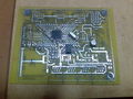
- over etching can cause a range of problems, even traces dissapear (see top left side of the picture);
- generally the traces are farily small and drill bits are farily wide in relation; its frequent that one drill hole in the middle of a trace can cut the trace off entirelly, or at least to reduce its trace considerably - anticipate and adress this issue both in pcb trace optimization and in soldering; moreover, in some cases with the soldering iron you will have easy access to only one side of that hole;
- its fairly common to forget to solder on both sides for some parts or pins, or even to make vias in wrong spots, etc.
- meter connections and triple check everything versus the pcb design files before plugging in.
Downloads for DIY toner transfer pcbs
Please note:
- these are NOT variations of the original designs, actually are exactly those! - only just pcb layout "tweaked" for toner transfer
- all credits and everything goes to the original authors
- all modifications were intended to be minimal, to preserve the original components positions, placements, traces etc, as much as possible, to ease any later debugging tasks. For the same reason, i choose (for myself) to have only the traces on the board no other polygons. This way i can see all traces clearly by putting the board into the light (i use a somewhat transparent cald). While this is not optimal for general pcb functioning (esp stepper drivers), it is a matter of choice - and the few images provided look like that as a result.
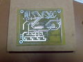
Image 1: ATX / ATX2 supply and UM232R footprint boards


- File download link: Zip Media:mtg_ttd_accesories.zip . For both boards, make sure you check the real parts (molex and module) fit on normal paper, before anything else. If the parts dont fit, print the file from an image editor program, at 600dpi, on A4 sheet setting in printer driver. Do not print from browser or from default windows image viewer.
- General device description: ATX / ATX2 voltages takeout + UM232R footprint board.
- Significant changes: No prior versions, only made these boards as alternatives. For ATX supply, the board allows access to all voltages without any modifications to the supply. The UM232R i made because it looks better on a proper board.
- Specific comments for DIY: Instead of soldering the UM232R module, .100 precision female header can be used to make a "socket" - use precision pins: these are the round ones.
Image 2: Motherboard 1.2v


- File download link: http://www.thingiverse.com/thing:4673
- General device description: Motherboard 1.2v
- Significant changes: Mb 1.2v: RepRap modifications included (no longer compatible with older makerbot version): the bridge near icsp header area, bridge(s) in atx connector area (leading to two traces in bottom layer to be combined on the top area of sd card - looks weird but its ok), tqfp pads are image edited.
- Specific comments for DIY: Additional image as A4 file, 600dpi, for top and bottm: orientation of the board on the file would of been better horizontal, but then wouldnt fit one near the other. Check photo paper shrinkage (on vertical direction) with a real piece of .100" pins along their holes.
Image 3: Extruder Controller 2.2v
- File download link: http://www.thingiverse.com/thing:4673
- General device description: Motherboard 1.2v + Extruder Controller 2.2v
- Significant changes: I did my own EC22 with a version that was almost at the size and spacings of the original file, and after doing it like that i decided it needs further spacing out and more severe cleaning up which i did in the file. As a result the images linked and the file are slightly different, and the last version should be better. However be warned, i did not tried this last version in real life myself, although i think it should work: use at your own risk, etc. Changes: tqfp pads image edited; layout enlarged; severe layout cleanup, many re-tracings; made connection between GNDA (analog gnd) and GND at the left of the crystal on top layer (instead of an alternate layer); as a sidenote, the brd file has the pin A6 (Aref, #20) placed a link to vcc just before C14 which is not clearly appearing in sch file, but seems to be correct.
- Specific comments for DIY: Additional image as A4 file, 600dpi, for top and bottm. Slightly complicated board with many vias, so make vias with the reference file on your face to avoid making wrong kind of via connections. Use good quality board and materials.
- Testing comments: testing the extruder without motor attached, but by turning pot to max resulted on my board in burning the top H-bridge, so in my opinion be carefull about that pot.
Optoendstops 3.0


- File download link: http://www.thingiverse.com/thing:4673
- General device description: optoendstops 3.0
- Significant changes: it should be failry easy to fit both smd or through hole components;
- Specific comments for DIY: has 4 pin header versus 3 pin headers on the stepper drivers; can be made single sided with 1 top layer wire bridge (but there is no reason for that);
StMoDrv 2.3v


- File download link: http://www.thingiverse.com/thing:3424
- General device description: This is the board layout made by mr. Renoir, documented on Thingiverse http://www.thingiverse.com/thing:3424
- Significant changes: Nothing. It is only mentioned here as a part of this "DIY" collection, i hope original poster wont mind.
- Specific comments for DIY: Refer to the original post on Thingiverse.
StMoDrv 3.0v


- File download link: http://www.thingiverse.com/thing:4673 (and there should be other peoples versions on thingverse aswell)
- General device description: at the time making this, it is the current version of RepRap Driver
- Significant changes: Nothing significant. Just traces width, etc.
- Specific comments for DIY: Image shows a socket for the plcc, because i intended to test it only. Would be wiser to solder the ic instead. Also: i havent actually got around to made it, so i cant say for sure that it works but i dont see why it shouldnt, as there were no changes that could raise this question. My best dilligence, but use at your own risk / keep that in mind.
StMoDrv 3.3v Makerbot


- File download link: http://www.thingiverse.com/thing:4673
- General device description: Version 3.3 of stepper driver, at the time making this page, in development set from makerbot (marked ready for production). It does not have the Optoendstops headers, has a 6 pin idc header and it added an reset line pin in it. Because the future mb will have min/max directly on it, which makes more sense.
- Significant changes: This came as an intermediate step in making the version below. More explanations there. Thought to put the file here for further reference maybe for makerbot diy users to do testing on it or maybe when a new mb will be available.
- Specific comments for DIY: Mostly same as below, read there.
StMoDrv 3.3v Mendel "pins compatible"

- File download link: http://www.thingiverse.com/thing:4673
- General device description: Same file as above, with 10 pin idc header and min/max headers for compatibility with Mb 1.2v, reset no longer connected to idc header for mb.
- Significant changes: changed smd from 0805 to 1206; increased pcb size and spacings accordingly; some provisions(”just in case”): 7805 can be fitted with a small to radiator and can be moved around abit if needed (also consider using 78L05 instead); smd versions electrolitic capacitors could be fitted (for smd connect the vias nearby with bottom layer); alternative jumpers instead of the dip switch; alternative 0.100” pins connectors for motor; 2 opposite diagonal holes for an eventual A3977 radiator, and some holes underneath A3977 that are just something like chip vent; should be easy to fit pots with 5/5mm pitch (instead of 5/2.5);
- Specific comments for DIY: Made a set of 3 with common supply lines and all seem to worke allright on first try. Because its "tuning" capabilities this 3.3v should be ideal for extruder so a set of 4 from start would make sense. If you plan to use smd versions C10 C11, may consider doing the nearby vias top connections only after populating these condensers. Underneath the a3977 i made some "venting" holes. I only use the traces so the pcb lacks alot of copper surface, as a result i would say serious overkill heatsinking on a3977 is in order (i used approx 40/35mm alu radiators). Fattening all traces with additional solder is good, especially on gnd lines - at least the ones entering the chip from top and below. Also, you may choose to use 78L05 regulator instead (~0.1A). The original 7805 (~1A) could make the board more likely to fry with a loose motor connection or ESD strike (quote from a comment in the page linked below).
- Usage / tuning for a certain motor: Mr. Nophead did some research on this board see this link http://hydraraptor.blogspot.com/2009/12/motoring-on-with-a3977.html (and linked pages). Also read 1)datasheet and 2)applications note sheet (link from allegro site FAQ of a3977), and understand basics of what Vref, Vpfd, Rc1 and Rc2 means and how they work.
Quick references (use at your own risk!):
Vref: this sets the max current (in value as half the voltage set), so take precautions: e.g. on a motor of 1,5A start tests with a smaller value, like 2V (thus 1A) and only if needed slightly increase until motor gets the desired torque, but without overshooting the motor rated Amps.
Vpfd: (voltage percent fast decay)- its voltage changes the decay mode e.g. 0-1.05V the decay is fast, and over 3V its slow decay, while in between these values its a mixed decay mode with more fast or more slow depending on which value the setting is closer to (how much slow and how much fast is a formula on app note sheet). Generally speaking fast decay ... is fast, but also gets more ripple and increases the heating, so bottom line: if the motor doesnt behave nicely with 100% fast decay, try mix mode decay in lower half of its interval, e.g. between 1.05-2V and see if improves.
RC1 and 2: values are adjusted in ohms not voltage, and should be identical at all times rc1=rc2. The CT values on this board is 470pF (C13 and C14). The rc values may need some "motor math" to discover proper values, see links above. I suspect a value from 42k - 56k would be a good place to start in most cases (motors with relatively acceptable low coil resistance - but not extreme), but ofc this cant hold true for all situations, so take the precautions needed in this area and review the proper documentation for it.
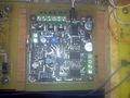
Photos
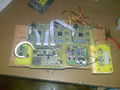
electronics -oe
electronics -oe, all tests ok
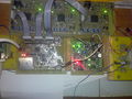
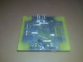
MB 1.2 in works top
MB 1.2 in works bottom
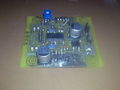
EC 2.2
StMoDrv 2.3v [made by Renoir]
StMoDrv 2.3v [made by Renoir]
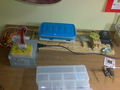
Horizontal sliding etching tank made from a garbage printer's carriage


Good links and further references
http://alternatezone.com/electronics/files/PCBDesignTutorialRevA.pdf
http://www.analog.com/library/analogDialogue/archives/39-09/layout.html
http://focus.ti.com/lit/an/szza009/szza009.pdf
http://code.rancidbacon.com/Electronics - page with further links, some about diy pcb
http://youtube.com - very good tips and examples of diy can be found here
Other Examples and other files
Following Reprap's attitude, please feel free to share more layouts related to reprap. Just a minimal template:
- File download link: ~
- General device description: ~
- Significant changes: ~
- Specific comments for DIY: ~