Generation 7 Electronics/pt
|
English • العربية • български • català • čeština • Deutsch • Ελληνικά • español • فارسی • français • hrvatski • magyar • italiano • română • 日本語 • 한국어 • lietuvių • Nederlands • norsk • polski • português • русский • Türkçe • українська • 中文(中国大陆) • 中文(台灣) • עברית • azərbaycanca • |
Release status: working
| Description | Generation 7 Electronics
|
| License | various - see individual boards
|
| Author | |
| Contributors | |
| Based-on | [[]]
|
| Categories | |
| CAD Models | |
| External Link | (none)
|
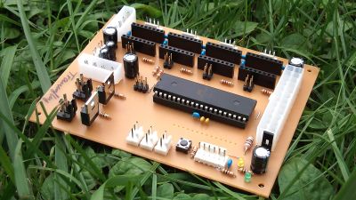
Este é um design eletrônico para RepRap concebido de forma que você possa faze-lo. A auto-replicação é o que faz da RepRap unica, agora isto extende-se para a parte eletrônica, todas as partes plasticas da Gen7 podem ser impressas na RepRap, em maquinas de fresagem CNC, gravada com o método de transferência de toner ou comprada. A meta para o futuro a longo prazo é para imprimir as faixas elétricas diretamente.
O design dos circuitos é muito semelhante a outras eletrônicas para reprap, como RAMPS or Sanguinololu. A Eletrônica Gen7 pode usar o mesmo hardware e firmware das outras. Além disso conta com alguns detalhes legais que tornam-o mais flexível e confiável..
- Assuntos sobre este projeto eletrônico Generation 7 Electronics forum thread.
- Faça o download dos arquivos Generation 7 Electronics GitHub repository. All the releases are tagged.
- Aqui os arquivos de fabricação latest release files folder.
Nota: A Eletrônica Generation 7 possui desenvolvimento e suporte contínuo de Traumflug. Sinta-se livre para fazer cópias do hardware para uso pessoal. Se quiser comprar comonentes para a Gen7, por favor vá até development supporting distribution channels. Obrigado.
Contents
Características e especificações
Destaques
- É Rápido! Roda a 20 MHz -> ganho de 25% em velocidade.
- É Completo! Cosegue controlar a base quente diretamente da paca.
- É Confortavel! Liga e desliga automaticamente.
- É Livre! Feita para a comunidade usar, desenvolver e distribuir.
- É Flexivel! Capaz de suprir o extrusor e a ase quente com diferentes voltagens.
- É Acessivel! Partes plasticas fáceis de fazer, imprimir na RepRap, ou comprar.
Detalhes
- Solução de placa unica.
- Placa impressa em apenas um lado.
- CPU: ATmega644, ATmega644P or ATmega1284P (Atmel Corp.)
- 4x drivers para motor de passo Pololu, adaptável, até micro-passo 1/16.
- Soldavel à mão, conversor USB-TTL on-board.
- Hardware integrado para um extrusor e para a base quente.
- Preferível fonte de alimentação: ATX 20-pinos or 24-pinos.
- Pode ligar e desligar a alimentação por software, mesmo usando uma fonte de alimentação ATX.
- Encaixe para extensão + Placas de extensão para extrusores adicionais, fans, cartões SD, ou o que for, é desejavel.
Metas de Design
- Manter a replicabilidade, i.e. distancia minima entre 2 trilhas de 0.4 mm. Esta é a regra para chips SMD.
- Ser independente de dispositivos industriais.
- Enfase na flexibilidade, fácil de usar e confiavel.
- Apenas o exencial na placa, partes adicionais em placas adicionais.
| Perfection (in design) is achieved not when there is nothing more to add, but rather when there is nothing more to take away. |
| A Perfeição(no design) não é alcançada quando não há mais nada a acrescentar, alcançada está quando não há mais nada a tirar. |
| Antoine de Saint-Exupéry - Tradução: "Dragão Heremita" |
Como Obter
Todas estas lojas dão suporte para o desenvolvimento da Gen7:
- RepRap DIY ( Traumflug's outlet )
- Paoparts
- eMotion Tech
Possuem placas impressas, componentes e conectores, alguns possuem kits.
Leia também as paginas wiki das placas individuais.
Individual Components
As Gen7 is a single board solution, it consists of only few components:
Board-AVR
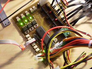
Gen7 Board is the central unit. It can drive a RepRap machine on its own, but not much more. Full power to the basics, no expensive extra features.
Latest Release: v1.5
20. December 2012
New features:
- The USB adapter is now on the main board. Pretty much what's on the ExtentionBoard-USB-B already, making this obsolete.
- Noise cancelling coil for AVcc now 10 uH. This makes Gen7 compatible with firmwares supporting LCD displays. Previously, hooking up a display would trigger the brown-out-detector often.
Future Release features
- Pulldown resistors for the MOSFETs (1 Mohms). Some people managed to overheat the MOSFET while experimenting with or even just uploading the firmware. Until this is done, please disconnect the heaters while playing with the firmware.
- Upp MOSFET LEDs to 1k5 to 2k2 for compatibility with 24 V.
- Jumper for M0? This would require a pulldown resistor in addition to the pullup one or M0 floats on A4983/A4988 based Pololus.
- Third power connector for even more juice for the heated bed?
- Couple the MCP2200's Reset to USB 5 V. This resets this chip when the USB cable gets disconnected, which fixes USB connection in some rare cases. See http://forums.reprap.org/read.php?181,63487,186725#msg-186725
- Plug for the reset switch to act as an emergency stop.
- 12 V onto the extension board connector for fans.
- Less tight track packing underneath the MCP2200. See discussion starting at http://forums.reprap.org/read.php?181,63487,218887#msg-218887
- Make auto-reset optional.
Board-ARM
Soon to come. Expected features:
- ARM LPC1114 Cortex-M0 CPU in a through hole pins package.
- 32-bit, 48 MHz.
- The unfortunate thing: firmware has yet to be ported.
Endstop
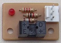
Gen7 Endstop 1.3.1 is an optical endstop, made to fit on Mendels & Co.
Extension Boards
Extension boards are what makes Gen7 powerful and feature rich. While the base board has only the essentials to get your printer running, you can add on this part later to enjoy all the goodies.
Here are a few extensions currently in development or already working:
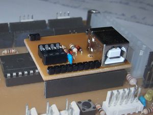
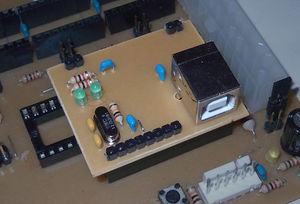
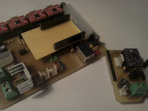
ExtensionBoard USB A: USB adapter using an ATtiny45/85
ExtensionBoard USB B: USB adapter using an MCP2200
ExtensionBoard 2E: Enhance your Gen7 with dual extrusion support
Xoan shows here how to design extension boards to allow stacking multiple ones.
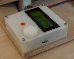
Gen7 ExtensionBoard LCD SD FAN by NightFly is an extension board with all the spiffy features people like: LCD, rotary encoder, fan connector, ...
Miscellaneous
Besides the parts needed for the individual components, you need thin wires to get the thermistor and end-stop signals to the Board. For example, you can salvage the cables you find between a PC main board and the PC's hard disks or those from any fans, indicator lights and reset switches.
Heaters and stepper motors need a bit more current, so the wires should be thicker. It's a good idea to use cables from mains household appliances. These have typically 2x or 3x 0.75 mm2 (~18 AWG) wire multi conductor cables. Remove the outer insulation carefully, and then re-group them in sets of two or four, as needed; twisting the wires while doing so reduces electromagnetic influence and keeps them tidy. Label the ends if you do not have enough colours, a permanent marker can be used to add a stripe to both ends of a wire, this lets you use one colour twice (and keep pairs matched up).
For shorter links or intermediate currents, the coloured wires from salvaged PC power supplies are well suited, sometimes they have two thicknesses on one PSU, you can strip the ends and compare which ones are the most suitable, they come in a number of colours, black, red, yellow and orange are the most common.
Assembly Instructions
As the wiring of the boards is slightly different for each released version, these details have been moved to the board's page.
Notice Regarding Legal Stuff
Generation 7 Electronics isn't a device in the sense of European Community regulation 2004/108/EG (EMC Directive). The reasons include:
- Gen7 doesn't include a power supply, so a Gen7 can't be used on it's own.
- Same for the stepper drivers. No stepper drivers, no useable Gen7.
- Heaters, thermistors, dito.
- The instructions seen on the Gen7 wiki pages give you hints on how to build your own device, they're not to be seen as installation instructions or a manual of a finished device.
If you use a Gen7 to assemble something usable, check (at least) the following if you want to conform to said regulation:
- Is there a metal housing? A Faraday Cage solves most electromagnetic issues.
- Connected cables can also be subject to electromagnetic stuff. Shielding them helps.
- Is there a manual and are there installation instructions conforming to the regulation?
If you buy and assemble an Generation 7 Electronics kit, you're manufacturer in the sense of the EMC Directive, not an end user. As long as you're developing and testing, most EMC regulations don't apply (for obvious reasons). The directive just wants you to protect devices of third parties from yours, so don't run a Gen7 right next to your neighbour's cardiac pacemaker. There's no time limit for developing and testing.
That said, this section mostly applies to all currently known RepRap electronics. Also, the said was written after investigation of relevant law texts by an mechanical engineer, not a lawyer.
Relevant law: EMVG, implementing the EC directive for Germany.
Development
Current status of development can be found at the Generation 7 Electronics GitHub repository. The short term goals are listed above in the #Releases section.
Layout, PCB Editing
Gen7 uses gEDA, a true open source set of Electronics Development Applications (EDA). While gEDA has a bit of a learning curve and has some room for improvement regarding the graphical user interface, it's reliable, fast and well suited for the task. gEDA is available for Linux and Mac OS X and has ready-to-use packages on Debian/Ubuntu and SuSe. To install it on Ubuntu, simply type
sudo apt-get install geda geda-utils geda-xgsch2pcb
and you'll find schematics and PCB layout editor applications in your applications menu.
Additionally, you want to download the design files with Git or GitHub's download button. In the later case choose to download source and unpack that when done.
Typical Work Loop with gEDA
Here you have a typical work loop for changing these electronics with the gEDA/PCB tool chain:
- Always start editing with the project (.gsch2pcb suffix) file. You can open it by double-clicking it.
- Select the schematics and use the button below the list to open it.
- When done, save it and return to the project.
- Open the PCB using one of the buttons to the right. Both have almost the same functionality.
- If you have chosen to update the PCB, footprints no longer in use will have vanished and new or previously missing ones appear in the upper left corner. An updated list of connections (netlist) will have been loaded. Update the rats nest to find areas requiring work.
- When done, save it and return to the project.
You get the idea?
Bug Fixing, Sending Changes
This is community development, so getting changes from everyone is more than welcome. Write them to the forum, to the reprap-dev mailing list, use GitHub's Issue Tracker, whatever is most convenient for you. If you fork the repository at GitHub, you can also send Traumflug pull requests.
PCB Manufacturing
gEDA can export PCBs to the Gerber and other file formats, of course.
Milling
On how to proceed further with that, see the PCB Milling page.
Etching
For etching, you likely want to reduce the amount of etched copper to a minimum. One way to get there perfectly, is to lay a ground plane into the layout.
Note: if you're in a hurry, you can leave out the step removing the tracks on the "GND-sldr" layer and setting Thermals. It'll work anyway.
- Open the layout in PCB.
- If you make a v1.4 board, find the Reset switch and see this one track on the "component" layer, connection the two bottom pins, usually in a greenish color. You'll come back to this track later.
- Hide the "component", "vias" and "pins/pads" layer by clicking on each of the colored rectangles in the layer list.
- Open Menu -> Window -> Netlist. It might be neccessary to pull the new window a bit taller to actually see the list.
- Click on the GND entry in the netlist (usually the third from top), then the "Select" button in the same window.
- Search for GND tracks touching square SMD pads. Use the Lock tool (tool buttons to the left) to lock them down.
- Choose Menu -> Edit -> Cut selection to buffer and click somewhere into the layout.
- Hit Esc on your keyboard.
- Unhide the three layers you hided before.
- By now, all tracks on the GND-sldr layer, usually the light blue ones, should have been removed. Vias and pins meant to connect GND, however, should be still there. Also GND tracks touching square pads should remain visible.
- Check the Reset switch, this one greenish track should be still there.
- Switch to the "GND-sldr" layer.
- Draw a RECT (find the tool in the left bar) as big as the entire board.
- Open Menu -> Window -> Message Log
- Do an "optimize rats nest" (o-key), watch the layout window for the yellowish rat lines and/or circles and watch the Message Log window for errors.
- Some non-GND tracks might be shortened with the new ground plane. Move the mouse over each of these tracks and press the "j" key (on your keyboard). Works for tracks hidden behind the ground plane as well, you'll see the difference immediately.
- For pins and pads you actually want to connect to the ground plane, set a Thermal (THRM tool to the left). The rat lines/circles will guide you which pins to connect to the GND plane. Thermals don't work for SMD pads, that's why we kept the regular tracks to them, before.
- It might be neccessary to add additional, smaller GND rects to reach areas not covered by the big rect.
- Loop the last four steps until you get congratulations (no errors) on "optimize rats nest" in the Message Log window. "Congratulations" means, your board's layout is connected correctly.
- In case the default clearance between the copper plane and pins/tracks are not sufficient for your purposes, you can adjust them with some command line work:
- Switch to the "solder" layer.
- Select Menu -> Edit -> Select all visible.
- Select Menu -> Windows -> Command Entry.
- Type the following and hit Enter:
ChangeClearSize(selectedlines, 0.5, mm)
- Repeat the above with
selectedpinsinstead ofselectedlines. - Repeat both of the above on the "Vcc-sldr" layer.
- As you probably guessed already, you can change this "0.5" to arbitrary values and "mm" to "mil", and use different values for each of the 4 groups.
- You're done.
On how to proceed with this etching-optimized board, see ... [Links needed]
Etching via Toner Transfer
Additionally to the above, the layout can be optimized for the toner transfer method even more:
- I'm not a real pro at toner transfer etching, so I generally oversize the traces and undersize the holes in the pads. This makes it more likely to get a good board. Toner transfer can be a bit of a pain. It is kitchen science in every way. Plus, since you are often drilling pads by hand it helps to oversize the pads too. Wider traces and smaller holes help the most. The wider traces help avoid open traces when etching is finished, and undersized holes helps avoid pads that etch too thin and are then liable to pop off the board when soldering. Also a smaller hole helps center the drill bit better.
Following up on this statement, the minimum track width was raised from 20 mil to 30 mil. As the minimum gap between copper is still 16 mil, other manufacturing processes shouldn't suffer from this. --Traumflug 20:33, 8 June 2011 (UTC)
You can reduce drill sizes with a few quick commands:
- Open the layout in PCB.
- Drag a rectangle over the entire board to select all elements.
- Select Menu -> Window -> Command Entry.
- Type the following two commands:
changedrillsize(selectedpins, 0.5, mm)
changedrillsize(selectedvias, 0.5, mm)
Voilá, all drills are reduced to 0.5 mm, just right to be a center hole for manual drilling.
Practical tips for toner transfer see DIY PCBs double sided toner transfer.
History
(Well, that part of the history which didn't result in a Release).
The Forum thread (german), where everything started.
Work Around Christmas 2010
Mostly done by Jacky2k.
24.12.2010: A first version of the Gen7 board has been etched and is being tested. The hardware seems to work, but the software still needs to be ported and tested with a RepRap.
29.12.2010: Some patches were made in the firmware to support endstops and homing. The patched firmware can be downloaded in the firmware section.
30.12.2010: Some more patches to the firmware. Current firmware seems to be stable and working. Not 100% tested yet.
04.01.2011: We found some bugs in the firmware again. All of them seems to be fixed, release is planned tomorrow.
05.01.2011: Uploaded current firmware with a lot of patches.
08.01.2011: Some little modifications of the PCB are required. Pull-up resistors for I²C are missing, we want to change some headers to more common one, some resistor values are missing, ...
09.02.2011: The master branch of FiveD on Arduino firmware is ported and seems to work but is not tested 100%. The config file for the firmware will come soon.
March 2011: Four Mendels are driven by Gen7 Electronics successfully, first reprap'd PCBs were shipped.
Older Releases
10. Feb 2011: v1.0
New features: it works. Isn't that the most important thing on an 1.0 release?
28. Mar 2011: v1.1
New features: fix all those silly 1.0 mistakes.
- Cleaned up that drill size mess. Now 275 of the 369 holes are either 0.75 mm or 1.0 mm, the remaining ones are the bigger ones for the connectors and can be drill-milled.
- Various smaller changes for better compatibility with G-Code generators.
- Added an appropriate plus (+) signs to all polar components.
- Swapped the TIP120 MOSFETs for IRFZ 44N ones. These are now fast enough to allow PWM in the kHz range.
- Added two jumper headers to one existing to have one for each of the three possible power sources. This adds safety against misconfigurations: use only one jumper and you're always safe.
- Fixed the solder mask.
- Changed the pin assignments of the heater MOSFETs. Now they're on PWM-able ATmega pins.
- Added a Release Maker script, bundling up design files for those without gEDA.
- Added Arduino Support, consisting of bootloaders, board descriptions and library files.
12. May 2011: v1.2
New features:
- The endstop now uses the TCST1103/2103 photo interrupter.
22. July 2011: 1.3
New features:
- Supported EDA toolchain is now gEDA 20100929, the one coming with Ubuntu 11.04.
- Use stronger 2 pin, 4 mm connectors (same type as the motors) for the heaters. These match the required current much better.
- Remove the MOSFET for the fan. Only few people use a fan. If you're one of them, connect the fan to the PSU directly.
- Remove the I2C header. Was totally unused.
- Make thermistor connectors 2 pin only. The extra pin just caused confusion.
- Replace the ATX20 with an ATX24. The new header is compatible with more recent PC power supply types and accepts ATX20 plugs just fine.
- Use another disk power type connector to supply the heaters. This allows to run a heated bed directly off the Gen7 board, without relays in between. This also introduces the ability to use different voltages for motors and heaters, without making things more complex for casual users.
- MOSFETs are now upright, for better cooling and mounting a heatsink. Also inserted a matching heatsink to the parts list.
16. August 2011: 1.3.1
This is a bugfix release.
- Attempt to prevent bootloader corruption by turning on the Brown Out Detector.
- Make the bootloader it's self a bit shorter.
- No changes to the hardware.
15. May 2012: Gen7Board v1.4
New features:
- Most important: Gen7 features now an extension header, so you can stack a feature-rich board on top of the base board. This shall allow for SD card support, additional extruders, displays and perhaps even multi-color extruders.
- Changed motor headers from KK156 to KK100 ones. KK156 are Gen3 and screw terminal compatible, KK100 are RAMPS/Sanguinololu/Gen6 compatible. The later are significantly cheaper and a lot more in use these days.
- Reduced the number of endstops to 3, so endstops no longer share pins with the ISP header. Additional endstops can go onto the extension board.
- Connect the thermistor to 5V Standby. This allows to read temperatures without turning the power supply on and requires just 0.1 mA additional juice at room temperature, so the additional energy needed for running the thing 24/7 is neglibile.
- Better GND routing for even more accurate temperature readings.
- Reduce resistors between ATmega and MOSFETs to 10 Ohms to allow for higher PWM frequencies.
- Tested support for the ATmega1284P.
August 2012: Gen7BR2
Diego Soares tweaked the Generation 7 electronics design, swapping out some of the connectors and other parts for parts that are easier to find in Brazil, producing the Gen7BR. RepRapBR - Grupo de Estudo: "Placa para RepRap Gen7BR2 - nacional" (RepRapBR - Study Group: "Board for RepRap Gen7BR2 - National")
17. August 2012: Gen7Board v1.4.1
New features:
- Distinction between extruder and bed circuitry (heater MOSFET, thermistor connection) to allow differences between them.
- Better MOSFET for the heated bed, bringing in more robustness and making MOSFET heatsinks obsolete.

