PhotoResistTransfer
Contents
Photo Resist Transfer Instructions
Tools You'll Need
| A UV lamp or UV lightbox (Maplins UV lamps part number L31AF) |
| A glass, ceramic, or plastic dish or tray in which to do the etching that can stand 100oC |
| Some mugs/jam-jars to mix the chemicals that can stand 100oC |
| A measuring jug |
| A reasonably accurate means of weighing chemicals (though you can get clever by weighing a lot on kitchen scales, then dividing the pile in half, then half again and so on). |
| A kettle |
| A small plastic sieve (a tea strainer is good) that can stand 100oC |
| A few small (< 5mm) glass, ceramic, or plastic beads that can stand 100oC |
| A funnel |
| Access to a good-quality laserprinter |
Consumables You'll Use
| Double-sided photo-resist PCB (for example from RS - part number 3970160) |
| Ferric chloride etchant (RS part number 551-277) |
| PCB developer (RS part number 690-849; sodium metasilicate) |
| Some overhead transparency sheets for a photocopier or laserprinter |
Alternatively you can buy a spray-can of photoresist and use that to prepare a plain double-sided board. The RS part number is 198-9651. This is probably only worth it if you are going to make a lot of PCBs - the spray has a best-before date that is sooner than a packet of biscuits...
What you are going to do
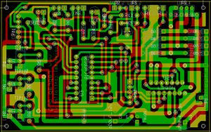
The example we will use is the Universal PCB that is used for both the RepRap motor controllers and the extruders. It is in the KiCad directory http://reprap.svn.sourceforge.net/viewvc/reprap/trunk/reprap/electronics/Universal-pcb/ The PCB looks like this in KiCad:
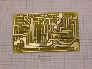
The red tracks are on the component side, and the green ones are on the reverse. Here is what you are going to make:
Printing and taping up the designs
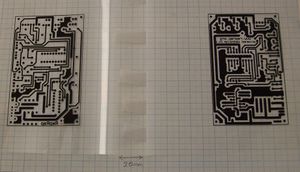
Download the the design. This is the "Copper" and "Component" postscript (.ps) or PDF files from the directory mentioned above. Use those files to print your own copy of the circuit design.
Print the files on overhead projector transparent sheets on a good-quality laserprinter (as mentioned above, inkjets don't produce a black enough print). The scale in the postscript files should be right, but check it as some print drivers rescale prints to fit them to their idea of a page. The simplest way to check is to hold the pins of an 18-pin DIP socket (which you'll need to put the PIC in) against the pads on the print where it will be located. The pins should fall exactly in the centres of the holes.
Cut about five 30 mm lengths of sticky tape and place them where you can get them.
Then cut about 20 mm off the long side of one of the prints. Put the two prints together toner-side to toner-side and get the circuits into registration. If you have a light-box this will help, but it is quite easy to do just resting them on a white sheet of paper. If (like mine) your close-up vision is blurred by the passing of the decades, use a magnifier to check that things are exactly aligned.
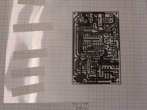
Without breaking the alignment, tape the cut sheet to the uncut one to make a hinge:
The tape, being clear, is not very clear... So here's what it looks like with the hinge unfolded:
Preparing and exposing the PCB
Leave the plastic covering on the double-sided photoresist PCB until you are ready to expose it.
Find a dark place to put the PCB after you have exposed it. I use a black document folder placed in a drawer.
Cut a rectangle of PCB 110 x 70 mm. This is larger than the finished result will be by about 5 mm all round. This will allow a margin so you can tape it down.
If the cutting has left burrs or raised edges remove them with a fine file.
Cut two 30 mm lengths of sticky tape and place them where you can get them.
If you expose the PCBs to visible light for a few tens of seconds while you are setting things up this doesn't matter; avoid sunlight (which contains UV).
Peel off the plastic protective film from both sides of the PCB, holding it by its edges. Try not to get fingerprints on the flat surface.
Place the PCB on the lower layer of the hinged transparencies so the design is central under it (close the hinge to check alignment), then tape it to the lower transparency, taking care to restrict the tape to the edges beyond the active area.
Expose the PCB to UV light on both sides. I have placed it under a sheet of glass (to flatten the transparency film right against it) under an old sun-tan lamp; that works well. Strong sunlight (beware clouds...) should do too.
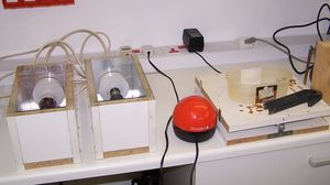
But best is a light box. These seem (for no good reason) to cost an absolute fortune, so I made two:
They are on the left. They are just aluminium-foil-lined chipboard boxes with the UV lamps from Maplins (part number L31AF) inside (thanks to my daughter, Sally, who gave me the components as a Christmas present - how can she have known?...). They have sheets of glass on top held by double-sided tape. On the right is a rocking tray for agitating the solutions during etching. That is more chipboard, driven by a crank from a small 60 RPM DC motor like the one used in the extruder. Note the professional-grade ice-cream tub for holding the etching chemicals, the plastic tongs for fishing out the PCB without dissolving one's fingers, and the ferric chloride stains (it gets everywhere...).
Place the transparencies with the PCB taped between them on the bottom box, invert the other box, and put it on top. You may need to add a scrap or two of waste PCB offcut between the glass to keep the glass sheets parallel.
With the materials and lamps listed above an exposure of 3 minutes 30 seconds seems to work well.
Back under the low light, untape the PCB and put it in its dark place.
Preparing the solution, and developing the PCB.
Get yourself organised - you really don't want to answer the phone while holding a beaker of sodium metasilicate solution.
Make up fresh solutions each time; saving used solutions in bottles is a false economy.
Fill the tray that you will use for developing and etching with water to a depth of about 20 mm. Pour that into the measuring jug to find the volume of each solution you will need.
Weigh out the sodium metasilicate developer. With the materials I specify above you need 25 g per litre (which is half the strength that it says on the developer bottle; the PCB specified uses half-strength developer).
Boil the kettle. Measure half the volume you will need of cold water into a jar (chemist's conical flasks are ideal for this if you can get them, incidentally), and top it up with the other half of boiling water. Dissolve the sodium metasilicate (which should dissolve quickly in the warm water). A glass stirring rod helps.
Pour the solution into your developing tray and put the beads in. The beads are to hold the PCB clear of the bottom so the solution can get to both sides. Put the PCB in and gently agitate it by rocking the tray.
You should see the exposed area of the photoresist dissolve into the solution, leaving the track pattern. Turn the PCB over after a while to check that both sides are developing.
When the results are clean, take the PCB out and run it under the tap to clean the solution off. If you have any, rinse it with a little distilled water (this will ensure no watermarks when it dries).
Pour the developer back into a jar through a sieve to separate the beads. Rinse the beads and tray under the tap.
You're Done! Now etch your board; instructions are here.
-- Main.ZachSmith - 12 Feb 2007
