MM PLD
This page is a development stub. Please enhance this page by adding information, cad files, nice big images, and well structured data!
Release status: Prototype
| Description | Fast prototyping tool for multiple material structures in the micrometer range
|
| License | |
| Author | |
| Contributors | |
| Based-on | [[]]
|
| Categories | |
| CAD Models | |
| External Link |
Multi-Material, Sequentially Masked Pulsed Laser Deposition
Motivation
Current micro and nanofabrication processes rely on a vast set of tools and technical capabilities, which usually implies a considerable capital expense and severely limits accessibility to such capabilities in many regions of the world. Small research organizations may acquire some of the tools required, but the fabrication process for standard devices require a substantial number of difficult and error-prone steps which take enormous amounts of know-how and optimization procedures in order to perform with an acceptable rate of success.
General Idea
The main goal is to generate an affordable, and easy to use system which allows the deposition of a wide range of materials in a geometrically controlled way, effectively enabling the creation of heterostructures with a wide range of functionality. Such a device may become a powerful tool for materials science research, and could also sustain interesting developments in distributed and participative manufacturing.
To implement such capabilities, the combination of the following techniques/ideas has been devised, with a particular twist ;)
Pulsed Laser Deposition
Pulsed Laser Deposition is a technique in which mass is transferred in a controlled atmosphere from a target to a substrate by means of irradiating the former with a high energy pulse of light. The energy transfered induces out of equilibrium thermal processes in the target, resulting in the formation of a plasma 'plume' which has a stoichiometry closely matched to the target composition.
While it's not the technique of choice for industrial device fabrication (mainly due to film quality and complications associated with large area deposition, see this section), the ability to deposit a wide range of materials has made it the workhorse for many research regarding complex materials (oxides, nitrates, dichalcogenides, etc) and the applications of some interesting effects (ferroelectricity, superconductivity, …) that they show. An often overlooked characteristic of this technique is the ease of coupling of the energy over the target: one can control with exquisite precision the amount, rate, placement an timing of the energy transferred from the laser.
A very comprehensive account of the technique is the book Pulsed Laser Deposition of Thin Films , while a more up to date account can be found in (TODO: references)
Shadow Mask Lithography
Stencil Lithography refers to the use of a usually solid mask with some defined apertures placed either in contact or some distance away from a substrate during a deposition process which effectively allows the spatially selective transfer of material. While this technique is seldom used in industry due to it’s practical resolution limitations, the spatial modulation of mass flow through an aperture is an inherently clean process which imposes very few limitations on the nature of the deposited species, as opposed to conventional resist based optical or e-beam lithography, where etching processes need to be carefully tailored to avoid undesired interactions, specially when there are underlying layers with very different physicochemical characteristics. It offers a series of benefits such as mask reusability, ease of manipulation, avoidance of resist contamination, loose constraints associated with substrate characteristics and the relative ease of implementation of dynamic lithography schemes, where the pattern moves with respect to the substrate allowing a grater deal of flexibility and some unprecedented capabilities regarding spatially tailored thickness and compositional variations.
Here are some reviews and relevant publications [1][2][ https://doi.org/10.3390/mi8040131]
The twist: Multimaterial PLD with sequential shadow masking
Now, while the ability to generate a patterned deposition is in itself quite useful, and a basic building block of any device integration, it`s still far away for the aforementioned objectives. But consider the possibility of being able to repeatedly perform such process with different materials and geometries, without breaking the controlled atmosphere nor requiring any manipulation of the substrate. This would enable, in principle, a completely bottom up approach to semiconductor (among other technologies) device fabrication.
There are indeed some articles describing similar ideas: check for example [3], [4], [5] or [6]. A more complete bibliography of related subject may be found on [7].
Now the proposed approach is based on something quite similar to roll to roll processing, but with the different masks riding on the web. Then one could use a standard multi-target carousel (mine was originally based on this design) to repeatedly deposit multiple structures in a single cycle.
The current approach uses a 30 micrometer thick aluminum foil as masking element, which is micromachined using a relatively inexpensive fiber laser marking machine [8], with a nominal resolution a bit over a micrometer. However, due to aspect ratio considerations, the mask apertures are limited to about 20 micrometers as a critical feature size. However, there are several resolution enhancement techniques which may be used to shrink the size of actual deposits. Here's an example, and the characteristics of the matter flow generated by PLD may lend themselves to quite novel schemes. (TODO: elaborate)
An example: Thin Film Transistor
So for illustrating how this may work, lets consider the fabrication of a bottom contacts, top gate thin film transistor. (This is of course a massive oversimplification of actual processes. The Art of Analog Layout by Alan Hastings is a quite friendly introduction, while Planar Process Primer is a bit more thorough. In any case, the technique is probably better suited for SOI devices.)
Basically we have 3 different materials arranged in 4 layers, each with its particular pattern. So in a standard fabrication flow, we may try something like this:(TODO)
While in the proposed system, we may load 3 different targets onto the carousel and use a set of masks which are moved in front of the substrate for each of the targets in the following way:
Implementation
So the first implementation was a modification of an existing system. Since I don't think the configuration was very hobbyist friendly, I will only document it briefly in MM PLD - v0. But I lost access to the vacuum chamber and laser, so a completely new iteration was needed.
Now the main advantage of being able to design a new chamber is that I could accommodate the system in such a way that machining the mask in-situ was possible. This has some important advantages:
  * The masking system is essentially self-aligned: as long as the sample and tape doesn't move, the mask pattern positional repeatability is only determined by the galvo system, which is designed by serious people
  * Corrections could be made on the fly
  * The actuation system becomes much simpler: No mask adjustments are needed, and if dynamic shadow masking is not desired, you only need that the tape       move on one direction.
But evidently it came with some tradeoffs:
   * Some particulates could fall over the substrate, messing the pattern transfer, and
   * The ablation in vacuum could produce a vapor phase (cool effect) which may coat windows (bad) and targets (worse)
Fortunately, the solutions to the aforementioned problems are considerably easier: You can keep the substrate relatively clean with a shutter 3, and the coating of different surfaces because of the mask machining could be hindered by an inert gas partial pressure.
PLD SAP: Main mechanism
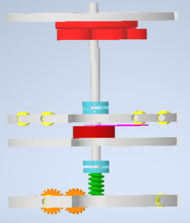
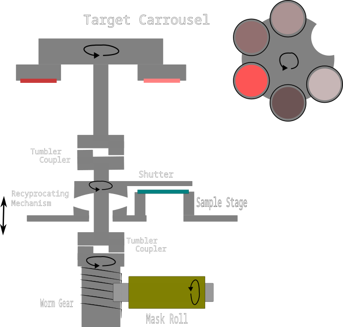
The system is based on a single rotary feedthrough which is coupled to the target carousel. It holds 5 25mm targets, and has an aperture to expose the mask to the beam for defining the apertures.
Now I've kind of copied a simple yet ingenious mechanism design shown in Warden, Robert M, 2006, which I found from this video. Its basically a rotational coupler with about 340 degrees of backlash, allowing oneself to disengage movement on any subsequent stage by rotation on the opposite direction. 4
So when the shutter is engaged, it rotates around the shaft and in certain positions push the 'sample stage' (which is kinematically mounted by a variant of the Kelvin Coupling) downwards a few millimeters, giving room for some clearance between mask and substrate.
Then, another coupler connects the shaft rotation with a worm gear which drives the tape mechanism.
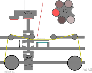
Therefore, the machine operation is roughly as follows:
* The shaft is rotated in a given direction, until the tape is translated enough to completely cover the substrate
* Changing the rotation direction, the shutter is placed between tape and substrate
* A valve isolates the high vacuum pump, and a certain pressure of inert gas is let onto the chamber. Then the mask apertures are micromachined according to the preestablished design.
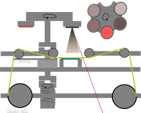
* When the mask is ready, the chamber is reevacuated (and possibly a particular atmosphere is set for the deposition). Then the shutter is moved back to a position where the substrate again in it's preestablished height.
* Changing direction again, the carousel is actuated to generate a given deposit from one or more targets sequentially, according to the layers needs. Then the process is repeated.


