A route for distributed electronics manufacturing ?
Posted by seumag
|
A route for distributed electronics manufacturing ? February 19, 2024 03:15PM |
Registered: 2 months ago Posts: 5 |
Hey, greetings to everyone.
I'm a physicist based on Santiago, Chile. During my degree I became interested in thin films and solid state technology, and by chance I ended up working with a deposition technique called pulsed laser deposition (PLD).
This may be a bit far fetched, but I was wondering if it may be of interest to someone on the community. Basically I've been working for a while on a variation of the aforementioned technique which may prove useful as a tool for quick prototyping for material deposition and device fabrication/integration. In particular I believe it may become a viable route for the distributed fabrication of integrated circuits and electronics components.
I've begun writing some documentation on the project PLD MM, for anyone interested.
To be brief, the idea is to use a relatively cheap laser engraver to generate a vapor phase out of solid targets in a vacuum or controlled atmosphere. The flow of matter is then modulated by a mask with apertures (stencil or shadow mask lithography) made out of metallic foil to generate a certain geometry over a substrate.
Now the relatively novel part is that the mask(s) are placed on top of a conveyor mechanism which allows the sequential deposition through many different masks. Add the capability to select the material which is ablated by the laser (which is quite trivial) and you could in principle generate complex devices without braking the vacuum or doing any external process to the substrate.
I've already generated a proof of concept based on a preexisting PLD system(which unfortunately I've lost access to before being able to generate functioning devices). Here's a small writeup.
Now I was a bit reticent to share that work before mainly because the equipment used wasn't widely available, but the new iteration is completely self funded and I've come to believe that it may possible to make a working machine with a reasonable budget. There are many hurdles and considerations to be taken into account for this kind of projects, I would love to have some input from the community, and will gladly discuss any ideas that may come up.
Best regards, SEU
Edited 1 time(s). Last edit at 02/19/2024 03:18PM by seumag.
I'm a physicist based on Santiago, Chile. During my degree I became interested in thin films and solid state technology, and by chance I ended up working with a deposition technique called pulsed laser deposition (PLD).
This may be a bit far fetched, but I was wondering if it may be of interest to someone on the community. Basically I've been working for a while on a variation of the aforementioned technique which may prove useful as a tool for quick prototyping for material deposition and device fabrication/integration. In particular I believe it may become a viable route for the distributed fabrication of integrated circuits and electronics components.
I've begun writing some documentation on the project PLD MM, for anyone interested.
To be brief, the idea is to use a relatively cheap laser engraver to generate a vapor phase out of solid targets in a vacuum or controlled atmosphere. The flow of matter is then modulated by a mask with apertures (stencil or shadow mask lithography) made out of metallic foil to generate a certain geometry over a substrate.
Now the relatively novel part is that the mask(s) are placed on top of a conveyor mechanism which allows the sequential deposition through many different masks. Add the capability to select the material which is ablated by the laser (which is quite trivial) and you could in principle generate complex devices without braking the vacuum or doing any external process to the substrate.

I've already generated a proof of concept based on a preexisting PLD system(which unfortunately I've lost access to before being able to generate functioning devices). Here's a small writeup.
Now I was a bit reticent to share that work before mainly because the equipment used wasn't widely available, but the new iteration is completely self funded and I've come to believe that it may possible to make a working machine with a reasonable budget. There are many hurdles and considerations to be taken into account for this kind of projects, I would love to have some input from the community, and will gladly discuss any ideas that may come up.
Best regards, SEU
Edited 1 time(s). Last edit at 02/19/2024 03:18PM by seumag.
|
Re: A route for distributed electronics manufacturing ? February 19, 2024 03:43PM |
Admin Registered: 16 years ago Posts: 13,891 |
... good work and thumbs up! 
What could be interesting for you too is the LIFT concept (Laser Induced Forward Transfer), which is pretty old/well known (since 30 years with lasers, since 50 years with focussed high energy light) and actually too used for micro-chip and sensors manufacturing.
Here one example site, to get a fast grip - [www.psi.ch]
It's using the same basis principle, but is more centered on "maskless" selective printing and some dynamic aspects of generating micro/nano-droplets out of a thin slice of paste or molten material.
What's pretty easy to accomplish, is some sort of "laser-assisted thermo-transfer" -- here some videos, where I've shown some of this with a paint coated glass plate:
[www.youtube.com]
[www.youtube.com]
[www.youtube.com]
Viktor
--------
Aufruf zum Projekt "Müll-freie Meere" - [reprap.org] -- Deutsche Facebook-Gruppe - [www.facebook.com]
Call for the project "garbage-free seas" - [reprap.org]
|
Re: A route for distributed electronics manufacturing ? February 19, 2024 04:11PM |
Registered: 2 months ago Posts: 5 |
Thanks!
Cool concept, I wasn't aware of it. The direct write approach should be even more flexible than the sequential masks, but probably thickness control would be a challenge. I'll look into it.
SEU
Quote
VDX
What could be interesting for you too is the LIFT concept (Laser Induced Forward Transfer), which is pretty old/well known (since 30 years with lasers, since 50 years with focussed high energy light) and actually too used for micro-chip and sensors manufacturing.
Here one example site, to get a fast grip - [www.psi.ch]
Cool concept, I wasn't aware of it. The direct write approach should be even more flexible than the sequential masks, but probably thickness control would be a challenge. I'll look into it.
SEU
|
Re: A route for distributed electronics manufacturing ? February 19, 2024 05:45PM |
Admin Registered: 16 years ago Posts: 13,891 |
... for better controllability of the thickness you can coat the "donator" plate with a thin layer of some micrometer thickness, an then control the transferred or recondensing surface thickness by the laser power - got some 10 to 100 nanometer target thickness out of 3 to 5 micronmeter thick donator sheet 
Viktor
--------
Aufruf zum Projekt "Müll-freie Meere" - [reprap.org] -- Deutsche Facebook-Gruppe - [www.facebook.com]
Call for the project "garbage-free seas" - [reprap.org]
Viktor
--------
Aufruf zum Projekt "Müll-freie Meere" - [reprap.org] -- Deutsche Facebook-Gruppe - [www.facebook.com]
Call for the project "garbage-free seas" - [reprap.org]
|
Re: A route for distributed electronics manufacturing ? February 19, 2024 08:00PM |
Registered: 2 months ago Posts: 5 |
My first though was repeatedly performing depositions which transfer a given thickness (which of course involved translating the 'donor'), but that's way simpler  .
.
I think the overall tech may actually be viable (I specially like the possibility of using a DMD to transfer a given geometry, like here). Still I wonder why this kind of ideas haven't generated a functioning machine, perhaps film (and therefore device) quality? I know that other routes for producing 'printed electronics' gathered quite a lot of interest some years ago (I'm thinking mostly solution based options, like this or the whole 'dektop fab' deal) but nowadays it doesn't seem such a hot topic.
Anyways, thanks for the tip. I'll keep working on the sequential mask approach, but an acquaintance is currently implementing a DMD based maskless litho machine (such as this one), I'll try to convince him that a LIFT mod could be fun 
.I think the overall tech may actually be viable (I specially like the possibility of using a DMD to transfer a given geometry, like here). Still I wonder why this kind of ideas haven't generated a functioning machine, perhaps film (and therefore device) quality? I know that other routes for producing 'printed electronics' gathered quite a lot of interest some years ago (I'm thinking mostly solution based options, like this or the whole 'dektop fab' deal) but nowadays it doesn't seem such a hot topic.
Anyways, thanks for the tip
. I'll keep working on the sequential mask approach, but an acquaintance is currently implementing a DMD based maskless litho machine (such as this one), I'll try to convince him that a LIFT mod could be fun
|
Re: A route for distributed electronics manufacturing ? February 20, 2024 04:47AM |
Admin Registered: 16 years ago Posts: 13,891 |
... DMD's are not long lasting enough for high power lasers or UV exposure - UV makes the plastic hinges of the micro-mirrors brittle, too high power will melt/wreck them with time ... best suited are galvos
Viktor
--------
Aufruf zum Projekt "Müll-freie Meere" - [reprap.org] -- Deutsche Facebook-Gruppe - [www.facebook.com]
Call for the project "garbage-free seas" - [reprap.org]
Viktor
--------
Aufruf zum Projekt "Müll-freie Meere" - [reprap.org] -- Deutsche Facebook-Gruppe - [www.facebook.com]
Call for the project "garbage-free seas" - [reprap.org]
|
Re: A route for distributed electronics manufacturing ? February 20, 2024 11:24AM |
Registered: 2 months ago Posts: 5 |
Not sure if it's totally uncompatible, at least regarding the micromirrors... damage threshhold from irradiation is usually dependent on peak power per unit area. If the laser hits the DMD uniformly and is then demagnified by say a 10x objective, then the difference in power density should be about two orders of magnitude. That could give you enough room to find settings where transfer is actually accomplished without significant damage... the hinges might be more troublesome though.
|
Re: A route for distributed electronics manufacturing ? February 20, 2024 12:05PM |
Admin Registered: 16 years ago Posts: 13,891 |
... I've got some "internal" numbers from Texas for life-span of their DMD's when exposed to UV radiation without UV-filter ... was then interested in using beamers for 3D-printing with UV-sensitive resins and 405nm LED's or 355nm lasers.
They stated some ten hours max., more like 2-4 hours
Viktor
--------
Aufruf zum Projekt "Müll-freie Meere" - [reprap.org] -- Deutsche Facebook-Gruppe - [www.facebook.com]
Call for the project "garbage-free seas" - [reprap.org]
They stated some ten hours max., more like 2-4 hours
Viktor
--------
Aufruf zum Projekt "Müll-freie Meere" - [reprap.org] -- Deutsche Facebook-Gruppe - [www.facebook.com]
Call for the project "garbage-free seas" - [reprap.org]
|
Re: A route for distributed electronics manufacturing ? March 03, 2024 08:15AM |
Registered: 2 months ago Posts: 5 |
Yeah, that doesn't seem like a sustainable route hehe. I suppose DMD based SLA printers use lower intensity, a high enough demagnification ratio could decrease the incident power density to safe levels...
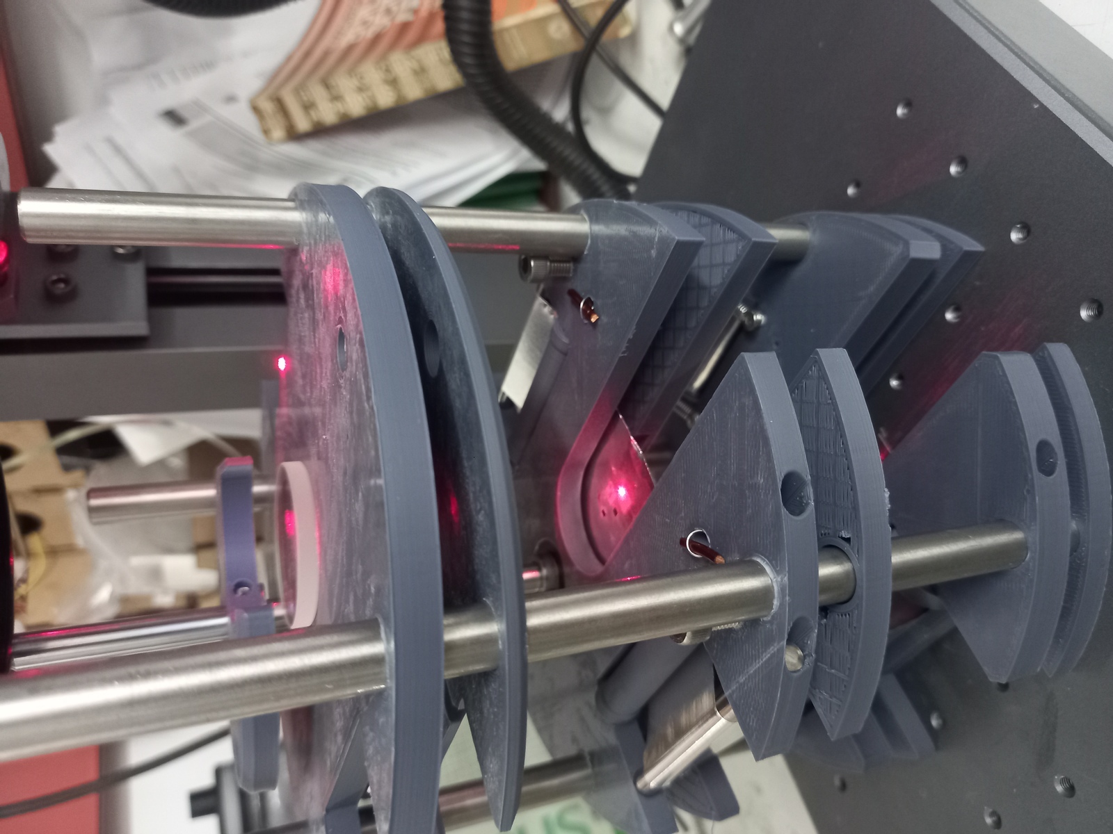
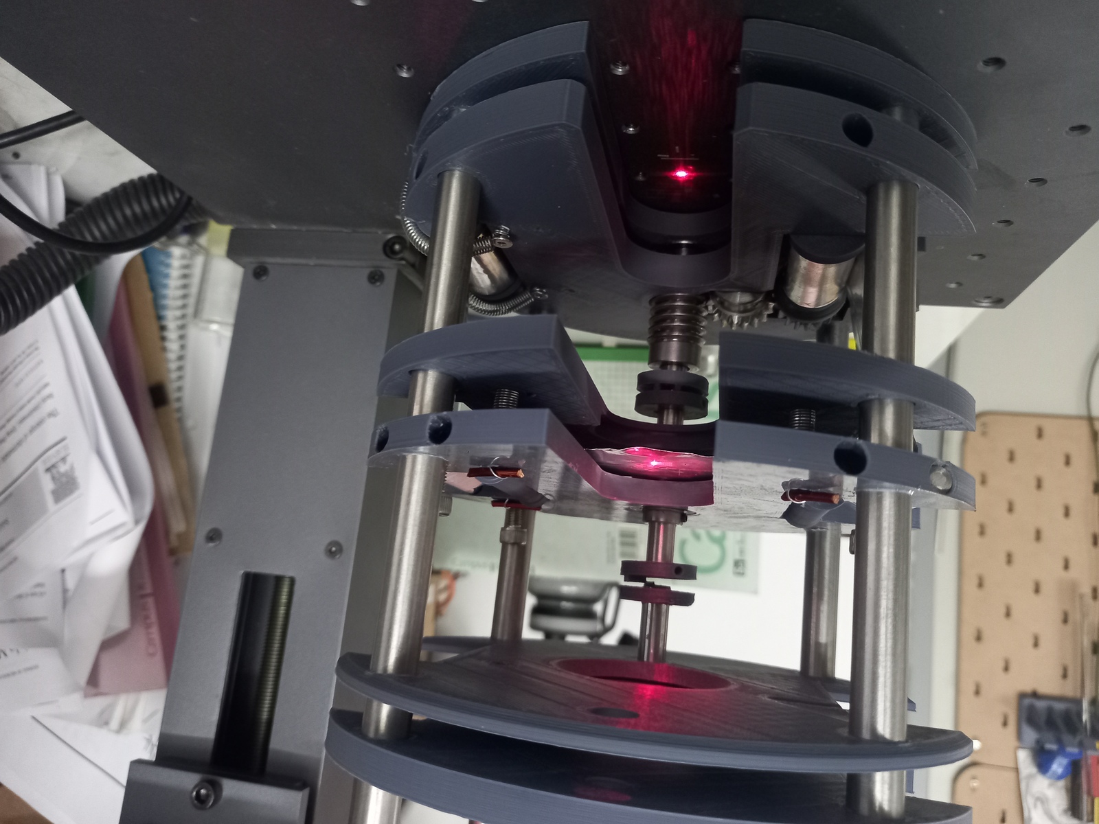
Anyways, some advances regarding the PLD system... the plastic prototype of the mechanism is working decently enough, and next week I regain access to a machine shop so the first iteration of the machine should be finished by the end of the month...
I'm a bit worried about the debris generated by the tape machining process, it's quite substantial and while it doesn't fall directly onto the substrate due to the shutter mechanism, it could clog previously defined apertures. Perhaps a slight flow of argon while machining could be enough to expel the particulates... or perhaps use a more substantial pressure differential after the process is complete could be used to 'vacuum' clean the tape.
Sorry, only registered users may post in this forum.